- This topic has 3 replies, 1 voice, and was last updated 4 years, 7 months ago by
.
-
Topic
-
What is the suitable gate drive circuits for MOSFET single phase Building and how to testing of gate drive circuits on bread board and then on PCB
What is the suitable gate drive circuits for MOSFET single phase Building and how to testing of gate drive circuits on bread board and then on PCB?
Viewing 3 replies - 1 through 3 (of 3 total)
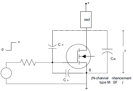 If the gate voltage is reduced to zero for turn-off operation, VDS attains the supply voltage magnitude (VDD), the potential at D swings from 0 to VDD and Cgd is charged up to to VDD (say, 100 V) through a low gate source impedance (Rg ) as shown in Figure below.
 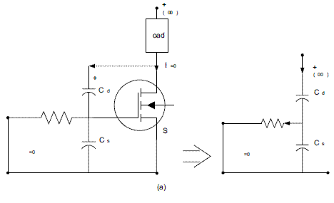 Now if a gate drive signal is applied (higher than the threshold value), the device will be on. Ideally, the voltage across D and S reduces to zero (neglecting small VDS) and terminal D will swing to ground potential (which earlier was at VDD . 100 V). The decreasing VDS produces a feedback current (i =Cgd . dVDS/dt) through Cgd to the gate circuit as shown in Figure below.
 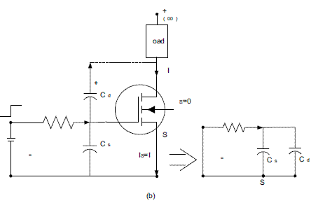 This feedback mechanism is called the
 Viewing 3 replies - 1 through 3 (of 3 total)
- You must be logged in to reply to this topic.