The input gate characteristics of a MOSFET differ from its bipolar counterparts. The gate is isolated electrically from the source by a layer of silicon dioxide. Ideally, no current flows into the gate when a dc voltage is applied. However, a small leakage current (of the order of 10-10 A) flows to maintain the gate voltage and also during the transition periods (off-to-on and on-to-off). Therefore, a small current is enough to charge and discharge the device capacitances. However, the device capacitances and gate-drive source impedance determine the device switching speed. There are three capacitances and they are nonlinear and voltage-dependent (Fig. below). 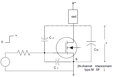 If the gate voltage is reduced to zero for turn-off operation, VDS attains the supply voltage magnitude (VDD), the potential at D swings from 0 to VDD and Cgd is charged up to to VDD (say, 100 V) through a low gate source impedance (Rg ) as shown in Figure below.
 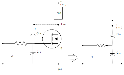 Now if a gate drive signal is applied (higher than the threshold value), the device will be on. Ideally, the voltage across D and S reduces to zero (neglecting small VDS) and terminal D will swing to ground potential (which earlier was at VDD . 100 V). The decreasing VDS produces a feedback current (i =Cgd . dVDS/dt) through Cgd to the gate circuit as shown in Figure below.
 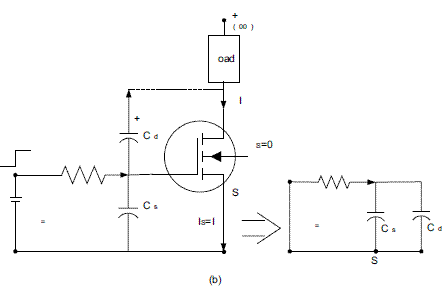 This feedback mechanism is called the