- This topic has 3 replies, 1 voice, and was last updated 4 years, 10 months ago by
Hamid.
-
CreatorTopic
-
2021-08-03 at 11:08 am #753
Ismail
I just want to know as fast as possible how to design power inverter using IGBT gate drive. I want to know the connections also and the diagrames.
I just want to know as fast as possible how to design power inverter using IGBT gate drive. I want to know the connections also and the diagrames. -
CreatorTopic
-
AuthorReplies
-
2021-08-03 at 11:08 am #2576
A normal ac inverter has three parts: 1. An input converter to rectify ac power to dc power. It is normally called the source bridge. 2. An energy storage device which separates the input from the output and allows each to operate independently from the other. It is usually called a link filter. 3. A dc-to-ac inverter in the output stage. It is called an inverter. It generates the desired ac output voltage and frequency. Pulse-Width-Modulated Inverters (PWM) is referred to as time ratio control. From a constant dc input voltage, we get a variable output voltage and frequency by varying the percentage of time that the power control switch is closed. The output voltage will increase by increasing the percentage of time the switch is closed. The switch is either open or closed. There is no power dissipation across the switch in both states.  Below figure illustrates a typical two-level PWM inverter circuit. It is similar to the SCR bridge, but it uses IGBTs for the switching devices. The energy storage capacitor is denoted by C. The motor connections are a, b, and c. The inverter operation is as follows: Once the output frequency required to satisfy the speed regulator is given to the control system, it calculates the three-phase voltage commands. A triangle voltage waveform is generated and synchronized with the desired IGBT switching frequency and phase. This is the PWM carrier waveform that sets the basic inverter switching frequency. The average width of the PWM waveforms generated approximates the sine wave reference. The inductances average and smooth the resulting waveform.
 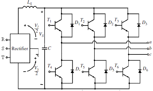 The IGBT is similar to the power transistor, except that it is controlled by the voltage applied to its gate rather than the current flowing into its base, as in power transistors. The current flowing in the gate of an IGBT is extremely small because the impedance of the control gate is very high. This device is equivalent to the combination of a metal-oxide semiconductor field effect transistor (MOSFET) and a power transistor (below Figure). Since the current required to control an IGBT is very small, it can be switched much more quickly than a power transistor. The IGBTs are normally used in high-power, high-frequency applications.
 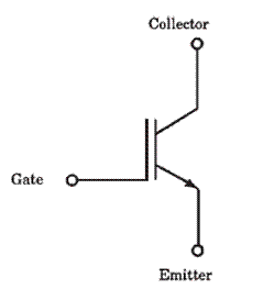 These bipolar power transistors are driven by an insulated gate metal-oxide transistor. A relatively simple 15-V gate driver signal is used to control the resulting high-current power transistor. The IGBT is a four-layer semiconductor similar to the SCR. Its main features are that 1. It has very fast switching on the order of 100 to 150 ns and resulting high-voltage transients dV/dt of 5000 to 10,000 V/?s. 2. The IGBT chips are soldered in place and connected with discrete bond wires. They are very weak when it comes to thermal fatigue problems. The IGBT modules have significantly lower thermal fatigue capability than other semiconductors. The high dV/dt generated leads to problems with bearing currents and the insulation system. Although thyristors, diodes, and IGBTs are solid-state devices, they have wear out mechanisms just as insulation and other mechanical parts do. The wear out and failure rates of these devices can be calculated. Common Failure Modes Differential Expansion (Mechanical Fatigue). This failure mode is mechanical fatigue or wear out caused by the difference in expansion rates as the temperature of the device changes. As the temperature of the device changes, different parts expand at different rates. These are the expansion coefficients for materials used in semiconductors:
 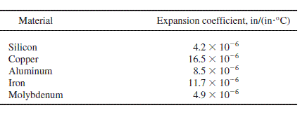 Thus, the parts slide over each other, causing mechanical wear out. This failure is common to all semiconductors. It normally occurs at the end of life of these devices. Below figure illustrates the general failure rate curve of SCRs, diodes, and IGBTs. The initial high failure rate is caused by manufacturing defects, application problems, and drive start-up stresses and lasts a few weeks. The high failure rate at the ends indicates the end of the life for the devices. In general, the lifetime of a device becomes shorter when it is operated harder and closer to its voltage rating.
 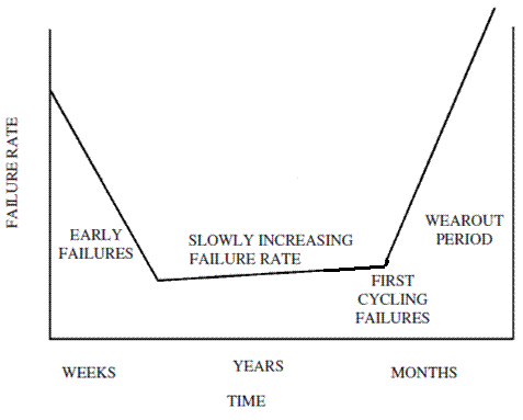 Fault Current Limit. This mode of failure is not applicable to IGBTs because they are not able to conduct currents in excess of their ratings. It is only applicable to thyristors and diodes GTOs. The junction temperature increases when the fault current increases. The maximum surge current that can be tolerated results in junction temperature excursion Tj of 3002021-08-03 at 11:08 am #2578
i want know more how to create a single phase power inverter. complete system with snubber circuit , gate drive circuit, heat sinks and powar switches.
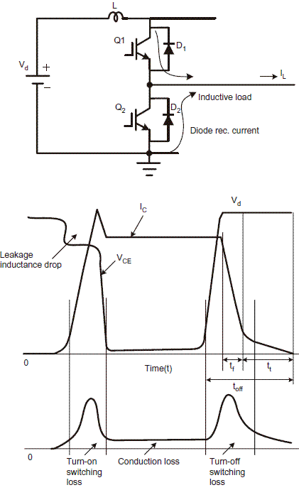
2021-08-03 at 11:08 am #2579A half-bridge voltage-fed IGBT inverter is shown in Figure, whereas Figure below shows the switching voltage and current waves when no snubbers are used (hard switched). Assume that the load is highly inductive and initially Q1 is off so that the lower diode D2 is carrying the full load current IL. When Q1 is turned on at t = 0, after a short delay time it starts to pick up the load current at full supply voltage (with a small leakage inductance drop) diverting D2 current. After D2 forward current goes to zero, current in Q1 consists of IL and D2 reverse recovery current (shown by the hump). When the recovery current is near the peak, the voltage of Q1 (VCE) falls to zero. When the turn-off gate signal is applied to Q1, its collector voltage begins to build up with a short delay at full collector current. When full voltage is built up across the device, D2 begins to pick up the load current. The short fall time (tf) and relatively long tail time (tt) of IC due to minority carrier storage of Q1 is shown in the figure. The SOA of the device is thermally limited like that of a MOSFET and there is no second breakdown effect. The conduction and switching loss curves, shown at the bottom of Figure, indicate that average switching loss will be high at high switching frequency. Note that the diode recovery current contributes significantly to the turn-on loss. Snubberless operation is possible but will cause high dv/dt and di/dt induced EMI problems. With a snubber, the turn-on di/dt and turn-off dv/dt will be slowed down, causing diversion of switching loss from the device to the snubber.
 A power integrated circuit is basically a monolithically integrated power and control circuit, sometimes with protection elements. Figure below, in contrast, illustrates a hybrid integrated circuit. Sometimes, a PIC is defined as an
 -
AuthorReplies
- You must be logged in to reply to this topic.